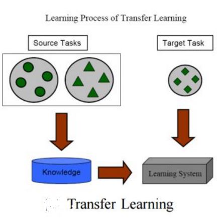
In material characterization, identifying defective areas on a material surface is fundamental. The conventional approach involves measuring the relevant physical properties point-by-point at the predetermined mesh grid points on the surface and determining the area at which the property does not reach the desired level. To identify defective areas more efficiently, we propose adaptive mapping methods in which measurement resources are used preferentially to detect the boundaries of defective areas. We interpret this problem as an active-learning (AL) of the level set estimation (LSE) problem. The goal of AL-based LSE is to determine the level set of the physical property function defined on the surface with as small number of measurements as possible. Furthermore, to handle the situations in which materials with similar specifications are repeatedly produced, we introduce a transfer learning approach so that the information of previously produced materials can be effectively utilized. As a proof-of-concept, we applied the proposed methods to the red-zone estimation problem of silicon wafers and demonstrated that we could identify the defective areas with significantly lower measurement costs than those of conventional methods.
翻译:在材料表征中,识别材料表面上的缺陷区域是至关重要的。传统方法涉及在预定的网格点上逐点测量相关物理特性,确定未达到期望水平的区域。为了更高效地识别缺陷区域,我们提出自适应映射方法,在此方法中优先使用测量资源来检测缺陷区域的边界。我们将这个问题解释为水平集估计问题的主动学习(AL)问题。AL-based LSE的目标是在尽可能少的测量次数下确定定义在表面上的物理特性函数的水平集。此外,为了处理重复生产类似规格的材料的情况,我们引入了转移学习方法,以便有效利用先前生产材料的信息。作为概念验证,我们将所提出的方法应用于硅晶圆的红区估计问题,并表明了我们可以比传统方法显著降低测量成本来识别缺陷区域。

