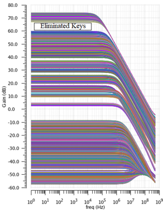
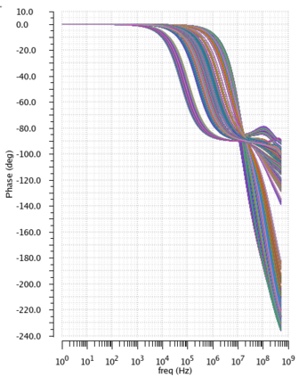
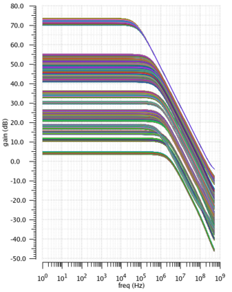
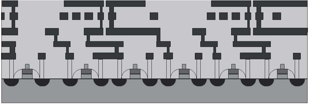
While numerous obfuscation techniques are available for securing digital assets in the digital domain, there has been a notable lack of focus on protecting Intellectual Property (IP) in the analog domain. This is primarily due to the relatively smaller footprint of analog components within an Integrated Circuit (IC), with the majority of the surface dedicated to digital elements. However, despite their smaller nature, analog components are highly valuable IP and warrant effective protection. In this paper, we present a groundbreaking method for safeguarding analog IP by harnessing layout-based effects that are typically considered undesirable in IC design. Specifically, we exploit the impact of Length of Oxide Diffusion and Well Proximity Effect on transistors to fine-tune critical parameters such as transconductance (gm) and threshold voltage (Vth). These parameters remain concealed behind key inputs, akin to the logic locking approach employed in digital ICs. Our research explores the application of layout-based effects in two commercial CMOS technologies, namely a 28nm and a 65nm node. To demonstrate the efficacy of our proposed technique, we implement it for locking an Operational Transconductance Amplifier. Extensive simulations are performed, evaluating the obfuscation strength by applying a large number of key sets (over 50,000 and 300,000). The results exhibit a significant degradation in performance metrics, such as open-loop gain (up to 130dB), phase margin (up to 50 degrees), 3dB bandwidth (approximately 2.5MHz), and power consumption (around 1mW) when incorrect keys are employed. Our findings highlight the advantages of our approach as well as the associated overhead.
翻译:暂无翻译


