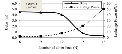
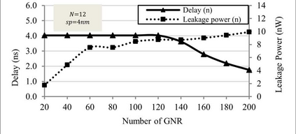
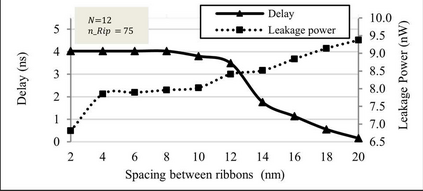
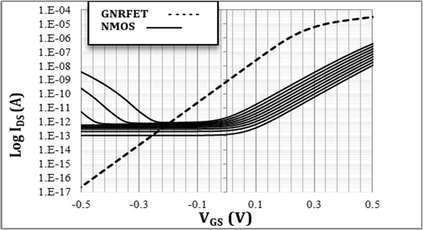
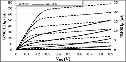
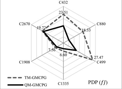
A robust power gating design using Graphene Nano-Ribbon Field Effect Transistors (GNRFET) is proposed using 16nm technology. The Power Gating (PG) structure is composed of GNRFET as a power switch and MOS power gated module. The proposed structure resolves the main drawbacks of the traditional PG design from the point of view increasing the propagation delay and wake-up time in low voltage regions. GNRFET/MOSFET Conjunction (GMC) is employed to build various structures of PG, GMCPG-SS and GMCPG-NS. In addition to exploiting it to build two multi-mode PG structures. Circuit analysis for CMOS power gated logic modules ISCAS85 benchmark of 16nm technology is used to evaluate the performance of the proposed GNR power switch is compared to the traditional MOS one. Leakage power, wake-up time and power delay product are used as performance circuit parameters for the evaluation.
翻译:提议采用16nm技术,使用Greagene Nano-Ribbon Field效应晶体管(GNRFET)进行强有力的电动格子设计;电动Gate(PG)结构由GNRFET作为电力开关和MOS动力门模块组成;拟议的结构从提高低电压区域传播延迟和觉醒时间的角度解决传统PG设计的主要缺点;GNRFET/MOSFET Concynction(GMC)用于建造PG、GMCPG-SS和GMCPG-NS的各种结构;除了利用它来建造两个多模PG结构外,还利用它来建造两个多模PG结构;对CMOS动力门逻辑模块ISCAS8516nm技术基准进行巡回分析,以评价拟议的GNR电源开关的性能与传统的MOS基准相比较。 渗漏能力、觉醒时间和力延迟产作为评价的性能路标参数。


